Unleash NOR Flash Performance: Synaptic Laboratories IP Maximizes DDR x8 Throughput on FPGAs

cropped SLL Revise 005 Wide 007 300dpi

In our world of embedded systems and configurable computing, fast and reliable boot times are paramount.

Increasingly, developers are turning to NOR flash memory for storing firmware, configuration data, and even application code intended for direct execution. While NOR flash offers advantages like non-volatility, random access, and code shadowing capabilities, achieving optimal performance, especially when dealing with complex data streams, can be a challenge. That’s where Synaptic Laboratories Ltd (SLL) comes in.

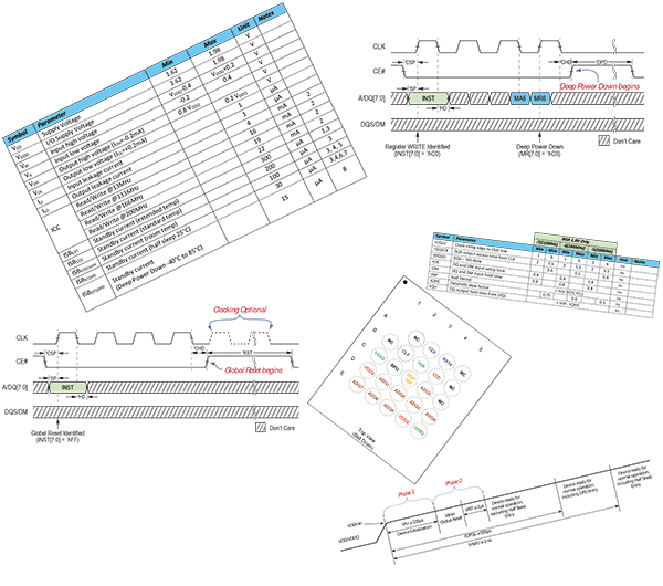
SLL has developed a groundbreaking Intellectual Property (IP) core specifically designed to unlock the full potential of high-speed NOR flash configurations within the fabric of an FPGA (Field-Programmable Gate Array). Their IP empowers developers to harness the exceptionally high throughput offered by a 200 MHz DDR (Double Data Rate) x8 configuration NOR flash, resulting in significantly improved run-time performance after system boot. This post will delve into the technical details, exploring the benefits of this SLL innovation and explaining why it’s becoming essential for applications demanding peak performance from their flash memory.

Understanding the Bottleneck: NOR Flash Performance Limitations

Traditional approaches to interfacing with NOR flash memory can often become a performance bottleneck. While the flash itself might boast impressive specifications, the interface logic implemented within an FPGA, without optimized IP, may struggle to keep pace. This can lead to suboptimal data transfer rates and ultimately impact overall system performance. Several factors contribute to this limitation:

  • FPGA Logic Complexity: Designing custom logic to handle complex NOR flash protocols, including DDR, requires significant FPGA resources and development time. This can be a costly endeavor, both in terms of time and silicon utilization.
  • Timing Constraints: Meeting the tight timing constraints required for high-speed DDR operations can be extremely challenging within the FPGA fabric. Factors like signal propagation delays and clock jitter can significantly impact data integrity and overall throughput.
  • Protocol Overhead: Standard NOR flash protocols often involve significant overhead, including address latching, command sequences, and wait states. This overhead can reduce the effective bandwidth available for data transfer.
  • Interrupt Latency: In many embedded systems, data transfer from NOR flash is triggered by interrupts. The latency associated with interrupt handling can further impact performance, especially when dealing with time-critical applications.

The SLL Advantage: Optimized IP for Peak NOR Flash Performance

Synaptic Laboratories Ltd.’s IP core addresses these challenges head-on, providing a pre-verified and highly optimized solution for interfacing with 200 MHz DDR x8 NOR flash memories within an FPGA. The core focuses on several key areas to maximize throughput and minimize latency:

  • High-Speed DDR Interface: The SLL IP is meticulously engineered to meet the stringent timing requirements of DDR operation. It leverages advanced FPGA features, such as dedicated I/O blocks and phase-locked loops (PLLs), to ensure accurate data capture and transmission at the specified 200 MHz clock rate. The x8 configuration further amplifies the throughput by transferring 8 bits of data per clock cycle.
  • Optimized Protocol Engine: The core incorporates a highly efficient protocol engine that minimizes overhead and streamlines data transfer. This engine intelligently manages address generation, command sequencing, and wait state insertion, ensuring that the flash memory is operating at its peak efficiency.
  • Configurable Memory Mapping: The IP core allows developers to configure the memory map according to their specific application requirements. This flexibility enables efficient memory management and reduces the need for complex address translation logic.
  • Advanced DMA Support: Integrated Direct Memory Access (DMA) functionality enables high-speed data transfer between the NOR flash memory and other peripherals or memory regions within the FPGA. DMA bypasses the CPU, significantly reducing processor load and improving overall system responsiveness.
  • Error Detection and Correction: The SLL IP incorporates error detection and correction mechanisms to ensure data integrity, especially in harsh environments where the risk of bit errors is higher. This feature enhances the reliability and robustness of the system.
  • FPGA Fabric Optimization: The IP core is designed to minimize resource utilization within the FPGA fabric. This allows developers to allocate more resources to other critical functions, such as signal processing or control logic.
  • Comprehensive Verification: SLL rigorously verifies its IP core to ensure its functionality and performance across a wide range of operating conditions. This extensive verification process provides developers with confidence in the reliability and robustness of the solution.

Benefits of Using SLL IP for NOR Flash Integration

The advantages of using SLL’s IP for integrating 200 MHz DDR x8 NOR flash memory into FPGA-based systems are numerous and impactful:

  • Increased Throughput: The primary benefit is a significant increase in data throughput compared to traditional NOR flash interfaces. This translates to faster boot times, improved run-time performance, and the ability to handle more demanding data streams.
  • Reduced Latency: The optimized protocol engine and DMA support minimize latency, resulting in faster response times and improved system responsiveness.
  • Simplified Development: The pre-verified IP core simplifies the development process, reducing the time and effort required to integrate NOR flash memory into the system.
  • Lower Development Costs: By using SLL’s IP, developers can avoid the costly and time-consuming process of designing custom logic for NOR flash interfacing.
  • Reduced FPGA Resource Utilization: The optimized IP core minimizes resource utilization within the FPGA fabric, allowing developers to allocate more resources to other critical functions.
  • Improved System Reliability: The error detection and correction mechanisms enhance the reliability and robustness of the system, ensuring data integrity.
  • Faster Time-to-Market: The availability of a pre-verified and highly optimized IP core enables developers to bring their products to market faster.
  • Scalability and Flexibility: The configurable memory mapping and DMA support provide the flexibility to adapt the IP core to a wide range of application requirements.

Applications Benefiting from Enhanced NOR Flash Performance

The SLL IP core is particularly well-suited for applications that demand high throughput and low latency from their NOR flash memory:

  • Embedded Systems: Faster boot times and improved run-time performance are critical for embedded systems, especially those used in real-time control and data acquisition applications.
  • Industrial Automation: Industrial automation systems often rely on NOR flash memory for storing configuration data and firmware. The SLL IP can significantly improve the performance of these systems, enabling faster response times and increased productivity.
  • Medical Devices: Medical devices often require fast boot times and reliable data storage. The SLL IP can help to ensure that these devices meet the stringent performance requirements of the medical industry.
  • Telecommunications: Telecommunications equipment often relies on NOR flash memory for storing firmware and configuration data. The SLL IP can significantly improve the performance of these systems, enabling faster data transfer rates and increased network capacity.
  • Aerospace and Defense: Aerospace and defense applications often require high-performance and reliable data storage. The SLL IP can help to ensure that these systems meet the stringent requirements of these industries.
  • Software Defined Radio (SDR): SDR applications often require the storage and retrieval of large amounts of data in real-time. Utilizing SLL’s IP for NOR Flash can drastically improve the performance of these applications.

Conclusion: SLL IP – A Key Enabler for High-Performance FPGA-Based Systems

In conclusion, Synaptic Laboratories Ltd.’s (SLL) IP core provides a powerful and efficient solution for unlocking the full potential of 200 MHz DDR x8 NOR flash memory within FPGA-based systems. By addressing the limitations of traditional NOR flash interfaces, the SLL IP enables developers to achieve significantly higher throughput, reduced latency, and improved overall system performance. Whether you are developing embedded systems, industrial automation equipment, medical devices, or telecommunications infrastructure, SLL’s IP can help you to unleash the power of NOR flash memory and create innovative, high-performance products. If you’re struggling to get the performance you need from your NOR Flash implementation, considering leveraging pre-verified IP from companies like SLL can save significant development time and resources, while ultimately leading to a superior product.

SLL is the only specialist, dedicated xSPI SIP design house since 2016. XSPI SIP design and support is SLL core business, for FPGA and ASIC. Visit our website to learn about SLL’s highly innovative xSPI SIP portfolio that is already successfully used by global customers including Fortune Global 500’s, and in 100m+ volume ASIC projects.

Synaptic Laboratories Redefines FPGA Configuration with High-Speed DDR NOR Flash Solution

cropped SLL Revise 005 Wide 007 300dpi

Synaptic Laboratories Ltd (SLL) has consistently proven itself a leader in technological innovation, and its latest breakthrough is no exception.

The company has recently announced a game-changing addition to its intellectual property (IP) portfolio: a novel solution that replaces the conventional, often sluggish, SPI (Serial Peripheral Interface) or QSPI (Quad SPI) configuration flash memory commonly used with Field-Programmable Gate Arrays (FPGAs). This new technology leverages a high-speed, low-pin-count, 200 MHz DDR (Double Data Rate) x8 NOR Flash, promising a significant leap forward in FPGA configuration performance and overall efficiency.

This blog post will delve into the details of this innovative solution, exploring its advantages, potential applications, and the impact it’s likely to have on the FPGA landscape. We’ll cover the limitations of existing SPI/QSPI solutions, the benefits offered by the DDR NOR Flash alternative, and the implications for designers and engineers working with FPGAs.

Understanding the Bottleneck: Limitations of SPI/QSPI Configuration Flash

FPGAs are incredibly versatile devices, offering the flexibility to be configured and reconfigured for a wide range of applications. However, this very strength – their programmability – hinges on the speed and efficiency of the configuration process. This process involves loading a bitstream (a file containing the configuration data) into the FPGA’s internal memory. Traditionally, this bitstream is stored in an external non-volatile memory like SPI or QSPI flash.

While SPI and QSPI have served as the de facto standard for FPGA configuration for years, they are not without their limitations:

  • Slow Configuration Times: SPI and QSPI are inherently serial communication protocols. They transmit data bit-by-bit, leading to relatively slow configuration times, especially for large bitstreams. This can be a significant bottleneck in applications that require rapid reconfiguration, such as dynamic reconfiguration systems or scenarios where boot-up time is critical.
  • Limited Bandwidth: The serial nature of SPI/QSPI also restricts the available bandwidth. This means that the rate at which data can be transferred from the flash memory to the FPGA is limited, impacting the overall performance of the system.
  • Pin Count Trade-offs: While SPI offers a low pin count (typically 4-6 pins), QSPI increases the bandwidth by using four data lines. However, this comes at the expense of increased pin count, which can be a constraint in space-sensitive applications.
  • Increased Power Consumption: The continuous serial data transfer in SPI/QSPI can contribute to higher power consumption compared to more efficient parallel data transfer methods. This is particularly relevant in power-constrained applications like mobile devices or battery-powered systems.
  • Software Overhead: SPI/QSPI communication requires dedicated drivers and software overhead, adding complexity to the overall system design.

These limitations become increasingly pronounced as FPGA designs grow more complex and the size of the bitstreams increase. The result is a bottleneck in the system, hindering performance and potentially limiting the applicability of FPGAs in certain demanding applications.

SLL’s Innovation: A High-Speed DDR NOR Flash Solution

Synaptic Laboratories has addressed these limitations head-on by developing a novel solution based on a high-speed, low-pin-count, 200 MHz DDR x8 NOR Flash. This approach offers a paradigm shift in FPGA configuration, providing significant performance advantages over traditional SPI/QSPI solutions.

Here’s a breakdown of the key features and benefits of SLL’s innovative solution:

  • DDR (Double Data Rate) Technology: Utilizing DDR technology doubles the effective data transfer rate compared to standard single data rate (SDR) flash memory operating at the same clock frequency. This significantly improves configuration speed and bandwidth.
  • 200 MHz Operating Frequency: The 200 MHz operating frequency further enhances the data transfer rate, allowing for rapid loading of the FPGA configuration bitstream.
  • x8 Data Bus Width: The x8 data bus width allows for parallel transfer of 8 bits of data simultaneously, significantly increasing the data throughput compared to the serial transfer of SPI/QSPI.
  • NOR Flash Memory: NOR flash offers byte-addressability, meaning individual bytes of data can be accessed directly without having to read an entire block. This facilitates faster and more efficient data access during configuration and other operations.
  • Low Pin Count: Despite the increased performance, SLL’s solution maintains a relatively low pin count, making it suitable for applications where space is a premium. This is crucial for integration into smaller form-factor devices and boards.
  • Simplified Hardware Design: The integration of DDR NOR flash can often simplify the overall hardware design compared to managing complex SPI/QSPI interfaces, potentially reducing development time and costs.
  • Reduced Latency: The faster data transfer rates and byte-addressability of NOR flash translate to reduced latency during configuration, leading to faster boot-up times and improved responsiveness.

Advantages of SLL’s DDR NOR Flash Configuration for FPGAs

The adoption of SLL’s high-speed DDR NOR Flash configuration solution brings a wealth of advantages to FPGA-based systems:

  • Dramatically Reduced Configuration Time: The primary benefit is a significant reduction in FPGA configuration time. This allows for faster boot-up times, quicker system initialization, and more responsive dynamic reconfiguration. This is particularly critical in applications like industrial automation, automotive systems, and high-performance computing where rapid startup or reconfiguration is essential.
  • Increased System Performance: Faster configuration times translate to improved overall system performance. FPGAs can be rapidly reconfigured to adapt to changing requirements, enabling more dynamic and efficient operation.
  • Improved Power Efficiency: While DDR technology itself can consume slightly more power, the significantly reduced configuration time means the system spends less time actively transferring data, potentially resulting in a net reduction in power consumption, especially in applications requiring frequent reconfiguration.
  • Enhanced Design Flexibility: The low pin count and simplified hardware design offer greater flexibility in system design, allowing engineers to optimize the placement of components and reduce board size.
  • Support for Larger Bitstreams: With the increased bandwidth, SLL’s solution can efficiently handle larger and more complex FPGA bitstreams, enabling the implementation of more sophisticated and feature-rich applications.
  • Potential for Over-the-Air (OTA) Updates: The increased bandwidth also makes it easier to implement Over-the-Air (OTA) updates of the FPGA configuration, allowing for remote bug fixes, feature enhancements, and performance optimizations without requiring physical access to the device.

Potential Applications and Industries Benefitting from SLL’s Innovation

The benefits of SLL’s high-speed DDR NOR Flash configuration solution are applicable across a wide range of industries and applications, including:

  • Telecommunications: Faster configuration times are crucial for rapid network reconfiguration and adaptation to changing traffic patterns in telecommunications infrastructure.
  • Automotive: ADAS (Advanced Driver-Assistance Systems) and autonomous driving applications require real-time processing and rapid adaptation to changing road conditions. SLL’s solution enables faster reconfiguration of the FPGA to handle these dynamic requirements.
  • Industrial Automation: Industrial robots and automated systems require rapid reconfiguration to adapt to different tasks and production lines. The faster configuration times provided by SLL’s solution can significantly improve throughput and efficiency.
  • Aerospace and Defense: High-performance signal processing and data acquisition systems in aerospace and defense applications demand rapid configuration and high bandwidth.
  • Medical Imaging: Medical imaging devices often require real-time processing and rapid reconfiguration to adapt to different imaging modalities and patient conditions.
  • Data Centers: FPGA-based accelerators in data centers can benefit from faster configuration times to optimize performance for specific workloads.
  • High-Performance Computing (HPC): Applications requiring dynamic reconfiguration of FPGA-based accelerators can benefit significantly from the reduced configuration latency.
  • Consumer Electronics: While cost considerations are paramount in consumer electronics, the improved boot-up times and power efficiency offered by SLL’s solution can be valuable in certain applications.

Conclusion: A New Era in FPGA Configuration

Synaptic Laboratories Ltd’s introduction of a high-speed DDR NOR Flash solution for FPGA configuration represents a significant step forward in FPGA technology. By overcoming the limitations of traditional SPI/QSPI flash memory, SLL has paved the way for faster configuration times, improved performance, and enhanced design flexibility. This innovation is poised to revolutionize the way FPGAs are used in a wide range of applications, empowering designers and engineers to create more powerful, efficient, and responsive systems. As FPGA designs continue to evolve and become more complex, solutions like SLL’s will become increasingly crucial for unlocking the full potential of these versatile devices. It will be interesting to see how this technology is adopted and how it influences the future of FPGA-based systems.

SLL is the only specialist, dedicated xSPI SIP design house since 2016. XSPI SIP design and support is SLL core business, for FPGA and ASIC. Visit our website to learn about SLL’s highly innovative xSPI SIP portfolio that is already successfully used by global customers including Fortune Global 500’s, and in 100m+ volume ASIC projects.

Navigating the Memory Maze: How the SLL xSPI Multiple Bus Memory Controller is Streamlining Embedded Systems

cropped SLL Revise 005 Wide 007 300dpi

As needs and technologies evolve in the  world of embedded systems, memory remains a critical cornerstone.

Its selection and efficient integration directly impact performance, power consumption, and the overall cost-effectiveness of a design. Choosing the right memory type, capacity, and interface is a complex balancing act. As demands for higher bandwidth and lower power continue to grow, traditional memory interfaces struggle to keep pace. This is where the emergence of xSPI-like memories and sophisticated controllers like the Synaptic Laboratories Ltd (SLL) xSPI Multiple Bus Memory Controller (MBMC) are revolutionizing the landscape.

This blog post delves into the importance of memory in embedded systems, explores the advantages of xSPI-like memories, and highlights the features and benefits that make the SLL xSPI MBMC a leading solution for interfacing with these advanced memories in both FPGA and ASIC environments.

The Vital Role of Memory in Embedded Systems

Embedded systems are ubiquitous, powering everything from smartwatches and IoT devices to complex industrial machinery and automotive control units. Regardless of the application, memory plays a fundamental role by providing:

  • Storage for Code: The embedded system’s firmware, operating system, and application software reside in memory. The performance of code execution is directly tied to the memory’s access speed and bandwidth.
  • Data Storage: Embedded systems often handle and process vast amounts of data, requiring ample memory to store sensor readings, configuration parameters, and temporary results.
  • Buffering and Caching: Memory acts as a buffer to smooth out data flow between different system components, mitigating latency and improving overall responsiveness. Caching techniques leverage faster memory regions to store frequently accessed data, further boosting performance.
  • Real-Time Operations: Many embedded systems operate in real-time, requiring deterministic and predictable memory access times. The choice of memory and its interface significantly affects the system’s ability to meet these strict timing constraints.

Therefore, the selection of memory is not a trivial task. It necessitates careful consideration of several factors, including:

  • Density: The amount of storage capacity required.
  • Speed: The access time and data transfer rate (bandwidth).
  • Power Consumption: Crucial for battery-powered and energy-sensitive applications.
  • Cost: Balancing performance with budgetary constraints.
  • Interface: The protocol used to communicate with the memory.
  • Reliability and Endurance: The lifespan and data retention characteristics.
  • Physical Size and Packaging: Important for space-constrained designs.

Limitations of Traditional Memory Interfaces

Traditional memory interfaces, such as parallel NOR and NAND flash, have served embedded systems well for many years. However, they face increasing limitations in meeting the demands of modern applications. Some of the key drawbacks include:

  • Low Bandwidth: Parallel interfaces require a large number of pins, increasing board complexity and cost. Even with wider data buses, achieving high bandwidth can be challenging due to signal integrity issues and timing constraints.
  • High Power Consumption: The parallel nature of these interfaces necessitates driving a large number of signals simultaneously, resulting in significant power consumption.
  • Large Footprint: The increased pin count translates to larger packages and larger board footprints, which is detrimental in space-constrained applications.
  • Complexity: Designing and implementing controllers for parallel memory interfaces can be complex, requiring specialized expertise and significant development effort.

Enter xSPI-like Memories: A New Paradigm

xSPI (eXpanded Serial Peripheral Interface) and similar serial protocols are emerging as a compelling alternative to overcome the limitations of traditional parallel interfaces. These protocols offer several advantages:

  • High Bandwidth: xSPI protocols can achieve significantly higher bandwidth compared to parallel interfaces by utilizing a smaller number of pins and operating at higher clock frequencies. Techniques like Double Data Rate (DDR) further enhance bandwidth.
  • Low Power Consumption: The reduced pin count and serial nature of xSPI minimize power consumption, making it ideal for battery-powered and energy-sensitive applications.
  • Small Footprint: The fewer pins result in smaller packages and reduced board footprint, enabling more compact designs.
  • Simplified Interface: While the underlying protocol might be complex, dedicated xSPI controllers abstract away much of the complexity, simplifying the integration process.

xSPI is not a single, rigidly defined standard. Instead, it refers to a family of serial protocols that share similar characteristics and objectives. These protocols often feature:

  • Single-Ended Signaling: Reducing cost and complexity compared to differential signaling.
  • Command/Address/Data Phase Separation: Streamlining the communication process.
  • Standardized Command Set: Facilitating interoperability between different vendors.
  • Scalable Bandwidth: Allowing for different operating modes and data bus widths (e.g., single, dual, quad, or octal) to adapt to different performance requirements.

Examples of xSPI-like memories include Octal SPI (OSPI) and HyperFlash, which are becoming increasingly popular in automotive, industrial, and consumer electronics applications.

The Synaptic Laboratories Ltd (SLL) xSPI MBMC: Your Gateway to Efficient Memory Integration

Interfacing with xSPI-like memories requires a dedicated controller that can handle the complexities of the protocol and provide a seamless interface to the host system. This is where the Synaptic Laboratories Ltd (SLL) xSPI Multiple Bus Memory Controller (MBMC) shines.

The SLL xSPI MBMC is a high-performance, configurable IP core designed to simplify the integration of xSPI-like memories in both FPGA and ASIC environments. It offers a wide range of features and benefits that make it a compelling choice for embedded system designers:

  • Comprehensive xSPI Support: The MBMC supports a wide range of xSPI-like protocols, including OSPI, HyperFlash, and other similar interfaces. This provides flexibility and future-proofing, allowing designers to choose the most appropriate memory for their application without being locked into a specific vendor or protocol.
  • High Performance: The MBMC is optimized for high bandwidth and low latency, enabling the embedded system to achieve its full performance potential. It supports various operating modes, including DDR and octal data bus widths, to maximize data transfer rates.
  • Configurability: The MBMC is highly configurable, allowing designers to tailor the controller to their specific needs. This includes configurable address spaces, command sets, timing parameters, and error handling mechanisms.
  • Multiple Bus Support: The “Multiple Bus” aspect of the name highlights a key feature: the MBMC can manage multiple xSPI memory devices simultaneously. This is crucial for applications requiring large memory capacities or parallel data access. The ability to interleave data across multiple memory devices significantly increases overall bandwidth.
  • AHB/AXI Interface: The MBMC provides a standard AHB (Advanced High-performance Bus) or AXI (Advanced eXtensible Interface) interface to the host system, simplifying integration into existing system-on-chip (SoC) architectures. These industry-standard interfaces ensure compatibility and ease of use.
  • Direct Memory Access (DMA) Support: The MBMC can be configured to support DMA, allowing data to be transferred between the memory and other system components without CPU intervention. This offloads the CPU and improves overall system performance.
  • Error Detection and Correction (ECC): The MBMC can be configured to support ECC, providing robust data protection and ensuring data integrity. This is particularly important in mission-critical applications where data corruption can have serious consequences.
  • Power Management Features: The MBMC incorporates various power management features, such as clock gating and power gating, to minimize power consumption. This is crucial for battery-powered and energy-sensitive applications.
  • FPGA and ASIC Implementation: The MBMC is available as both a soft IP core for FPGA implementation and a hard IP core for ASIC implementation. This provides flexibility and allows designers to choose the most appropriate implementation technology for their application.
  • Comprehensive Documentation and Support: Synaptic Laboratories Ltd provides comprehensive documentation and support for the MBMC, making it easy for designers to integrate and use the controller effectively.

Benefits of Using the SLL xSPI MBMC

Choosing the SLL xSPI MBMC offers several significant benefits:

  • Reduced Development Time: The MBMC simplifies the integration of xSPI-like memories, reducing development time and effort. Designers can focus on their core application logic rather than spending time developing and debugging complex memory controllers.
  • Improved Performance: The MBMC’s high-performance architecture and configurable features enable the embedded system to achieve its full performance potential.
  • Lower Power Consumption: The MBMC’s power management features minimize power consumption, extending battery life and reducing energy costs.
  • Reduced System Cost: The MBMC’s simplified interface and efficient design can help to reduce system cost by minimizing the number of components required and reducing board complexity.
  • Increased Reliability: The MBMC’s ECC support and robust design ensure data integrity and increase system reliability.
  • Future-Proof Design: The MBMC’s support for a wide range of xSPI-like protocols provides flexibility and future-proofing, allowing designers to easily adapt to new memory technologies as they emerge.

Conclusion: Embracing the Future of Embedded Memory Interfaces

The increasing demands of modern embedded systems necessitate the adoption of advanced memory technologies and efficient interface solutions. xSPI-like memories are emerging as a powerful alternative to traditional parallel interfaces, offering significant advantages in terms of bandwidth, power consumption, and footprint.

The Synaptic Laboratories Ltd (SLL) xSPI Multiple Bus Memory Controller (MBMC) is a leading solution for interfacing with these advanced memories, providing a comprehensive set of features and benefits that simplify integration, improve performance, and reduce system cost. By embracing the MBMC, embedded system designers can unlock the full potential of xSPI-like memories and create more powerful, efficient, and reliable embedded systems. As xSPI adoption continues to grow, the SLL xSPI MBMC is poised to become the de facto standard for interfacing with these memories in both FPGA and ASIC environments, paving the way for the next generation of embedded devices.

SLL is the only specialist, dedicated xSPI SIP design house since 2016. XSPI SIP design and support is SLL core business, for FPGA and ASIC. Visit our website to learn about SLL’s highly innovative xSPI SIP portfolio that is already successfully used by global customers including Fortune Global 500’s, and in 100m+ volume ASIC projects.